|
This article focuses to general principles of CCD detectors, their
physical characteristics influencing CCD imaging (like thermal noise)
and basic procedures dealing with unlovely effects (like elimination
or at last reduction of thermal noise). Those with some experience
with CCD cameras—observers who understands why
the raw CCD images must be calibrated (at last “dark frame”
should be subtracted, ideally also “flat field” should be
applied)—need not to read it.
However, this article is not intended for thorough explanation of
all CCD solid state detector operation principles. This topic is well
described in number of books and also some companies publish PDF
document covering this topic (e.g. ccdPrimer1 and ccdPrimer2
application notes published on Kodak web site).
Charge-Coupled Devices (CCDs)
CCDs originated its life as experimental computer memories, but
their capability to convert incoming light into electrical charge
made them the best solid state light detectors. The basic
operation principle is rather simple—incoming light creates electrical charge (electron
particles) in the silicon chip. Free electrons cannot travel
through the chip freely, because the chip is designed so the grid
of negative potential walls (stripes on the chip with negative
charge, which repel electrons) and electrodes (conductors also
polarized with negative voltage and thus repelling electrons) keep
them in areas called potential wells. Each potential well
represents one pixel (“pixel” is an abbreviation for
“picture element”—the smallest
“square” in image). Number of pixel in horizontal and
vertical direction as well as physical dimensions of one pixel
comprise basic CCD characteristics. Pixels more exposed to light
contains more electrons and vice versa. Here comes the big
advantage of CCD over human's eye: charge can be accumulated in
pixels, thus CCDs can detect light from very dim sources simply by
accumulating light-generated electrons over a long time.
As was already said, CCD silicon chip is covered by a structure
of electrodes, which keep light-generated electrons in pixels. But
the electrode structure is somewhat more complex. By applying
various voltages to various electrodes, electrons can be poured
from one well to the neighboring well. So it is possible to shift
the charge over a chip area. This process is used when it is
necessary to read the image from CCD. Chunks of electrons,
representing individual pixels, are shifted to the CCD output
node, where the electrical charge is converted into electrical
voltage. This voltage appears on the CCD output pin. The camera
electronics then measures the voltage (converts the voltage to
number using ADC—Analog to Digital
Converter) of each pixel. Information about charge accumulated in
each pixel (number representing number of electrons and thus
number of detected photons) then creates image data file.
Pixels can be organized several ways:
A single row of pixels comprise linear CCD.
Linear CCDs can be used when only one-dimensional image is
needed (e.g. while obtaining the spectra, which are
one-dimensional in principle). However, full two-dimensional
image can be created with linear CCD during a period of
time—it is enough when the detector and
the target object moves relative to each other and image is
scanned line by line. This principle is used e.g. in document
scanner, which scan line by line while the detector and its
optics moves under the document. Also cameras used in orbiting
spacecrafts often use linear detectors, read in time
intervals—the orbital motion of the
spacecraft is used to accumulate planetary surface image line by
line. Pixels arranged into a matrix on a silicon chip comprise
array CCD. Array CCD detects an image at once. They are
used in video and still cameras and also in astronomical CCD
cameras. Pixels accumulating light are organized into
columns in area CCDs. Applying appropriate voltage to vertical
electrodes shifts whole image (all pixels) along columns one row
down. This means all image rows move to the next row, only the
bottom-most row moves to so-called horizontal register.
Horizontal register can be then shifted by horizontal electrodes
to the output node pixel by pixel. Reading of array CCD means
vertical shifts interlaced with horizontal register shifts and
pixel digitization.
Even array CCDs can have various design: | Full Frame (FF) | devices expose all its area to light. It is necessary to
use mechanical shutter to cover the chip from incoming light
during readout process else the incoming light can smear the
image. FF devices are best suited for astronomy tasks, because
they use maximum area to collect light. Devices with really high
QE are always FF devices. 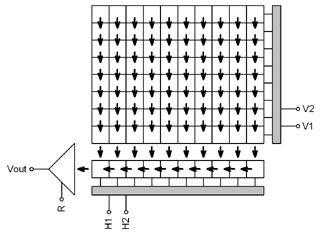
Full Frame sensor (number of horizontal and
vertical clock pins differ depending on CCD
architecture) 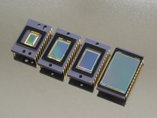
Kodak Full Frame CCDs: KAF-0402ME, KAF-1603ME,
KAF-3200ME and KAF-6303E | | Frame Transfer (FT) | devices comprise two areas, one exposed to light (Imaging
Area—IA) and second covered by opaque
coating (Storage Area—SA). When the
exposition finishes, image is very quickly transferred from IA
to SA. The SA then can be relatively slowly digitized without
smearing the image by incoming light. This feature is sometimes
called electronic shuttering. But such kind of shuttering also
have some limitations. First it does not allow to expose dark
frames—camera must be equipped with
mechanical shutter either way to automatically obtain dark
frames without bothering the observer to manually cover the
telescope. Second, although the SA is shielded from the incoming
light, charge can leak to SA from IA during slow digitization
when imaging bright objects (e.g. Moon). Important
negative side of FT is its price. Manufacturing large silicon
chips without faulty pixels is an expensive task and FT chips
must be two times the size of the IA. This is why companies are
abandoning production of FT chips. | | Interline Transfer (IT) | devices work similarly to FT devices (they are also
equipped with electronic shutter), but their storage area is
interlaced with image area. Only odd columns accumulate light,
even columns are covered by opaque shields. Odd columns are
quickly transferred to even columns on the end of exposition,
even columns are then shifted down to horizontal register and
digitized. 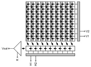
Progressive Interline Transfer sensor Interlacing of image and storage columns limits
the light-collecting area of the chip. This negative effect can
be partially eliminated by advanced manufacturing technologies
(like microlensing) described later. The television signal
does not contain simple sequence of individual frames from
historical reasons. It rather consists of interlacing images
containing only half rows, so called half-frames. The odd
half-frame contains rows 1, 3, 5 etc., the even half-frame
contains rows 2, 4, 6, etc. Companies producing CCD sensors
followed this convention and created CCD chips for usage in TV
cameras, which also read only half-frames. But if only
half of rows is read and the second half is dumped, the CCD
sensitivity would decrease by 50%. This is why the classical
“TV” CCD sensors electronically sums (see Pixel binning)
neighboring rows so that the odd half-frame begins with single
1st row, followed by sum of 2nd and
3rd rows, then by sum of 4th and
5th rows etc. The even half-frame contains sum of
1st and 2nd row, followed by sum of
3rd a 4th rows etc. 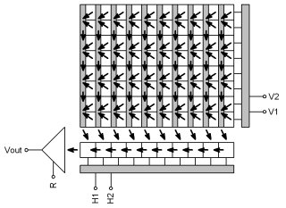
Interlaced Interline Transfer sensor (even
half-frame read) CCDs using this architecture are called
interlaced read sensors, as opposite to sensors capable
to read all pixels at once, called progressive read
sensors. Despite the implementation of micro-lenses, the
opaque columns reduces the quantum efficiency of IT CCDs
compared to FF ones. If the sensor dynamics range should not be
limited, the opaque columns must be of the same width as the
active ones. There is a combination of both interlaced and
progressive architectures, which allows narrowing of opaque
columns and thus boosting of the chip sensitivity. Such CCDs are
called frame read CCDs—each two
pixels in adjacent rows shares one pixel in opaque column, which
then can be only half as wide, because each pixel is two times
high. The pixel area and also its dynamic range remains the
same. Individual rows are not summed during frame read, but odd
and even half-frames are read sequentially. Let us note
that this way of CCD read requires using of mechanical
shutter—pixels of the even half-frame
ere exposed during odd half-frame read. Frame readout CCDs are
often used in digital still cameras. |
Chip QE is influenced by number of manufacturing
technologies:
The negative shielding effect of electrodes on the chip
surface can be reduced by using more transparent
material. Manufacturers can create a small lenses above every
pixel. Such lens focus light from insensitive chip areas (e.g.
covered by electrodes) to sensitive areas, where light is not
wasted. Especially Interline Transfer devices use microlenses to
eliminate the effect of opaque columns in the imaging area. But
also FF devices can benefit from microlenses applied above
pixels to increase overall QE. The best possible QE is achieved by thinned,
back-illuminated chips. The chip is packaged
“upside-down”, so electrodes and all shielding armature
appears on the bottom side of the chip. The chip is then thinned
to be very slim. All chip area then collects light. But
production of back-illuminated chips is expensive and such chips
can also introduce some negative effects, like occurrence of
interference figures caused by atmospheric IR radiation
etc.
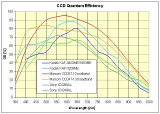
Quantum efficiency of some popular CCDs But the image quality is determined by the resulting signal to
noise ratio, not only by the pure quantum efficiency. For instance
two times better QE and four times bigger noise results to two
times worse S/N ratio. That means a slightly less sensitive chip
with low thermal noise can deliver better results than
comparatively cooled high-sensitive chip with bigger thermal
noise.
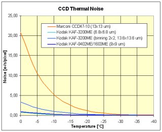
Typical dark current (in e-/s/pixel) for
back-illuminated Marconi CCD47-10 and front-illuminated Kodak
KAF-3200ME and KAF-1603ME Although the KAF-3200ME front-illuminated CCD has slightly
lower integral quantum efficiency than back-illuminated Marconi
CCD47-10, it has about 1/12 dark current at -25 °C. Even if the
KAF-3200ME is used in 2 × 2 binned
mode to achieve similar pixel size (13.6 μm vs. 13 μm), the dark signal
remains 3× lower compared to back
illuminated chip at this temperature. It is necessary to cool down
the CCDs to about -45 °C to achieve similar dark noise.
Pixel binning
Let us note one feature of CCD chips often used in
astronomy—individual pixels can be
electronically binned. It is possible to pour charge from
one pixel into another before the target pixel is emptied. The
charge in the target pixel then represents illumination of two
pixels. It is possible to bin pixels vertically by shifting of two
image rows into horizontal register without reading it after the
first shift. It is also possible to bin pixels horizontally by
shifting horizontal register two times into output node without
resetting it after the first shift. Combining of both vertical and
horizontal binning leads to square (or rectangular) image binning.
For example 2 × 2 binning is a
combination of 2× vertical and
2× horizontal binning. Then number
of binned pixels is usually limited by the camera electronics and
firmware. Some cameras allow for only a few predefined binnings,
e.g. 2 × 2 and 3 × 3. Some cameras are capable to bin image in a
predefined ranges, e.g. any combination of 1–4 in horizontal and 1–16 in vertical direction.
What is the reason for reading binned images? The resolution of
image (number of pixels) is lowered and the sensitivity is
increased. Binning is very useful e.g. if the camera pixels are
much smaller than the smallest detail the telescope can create, be
it due to bad seeing, long focal length etc. Binning then
increases the pixel size and enhances sensitivity without loosing
angular resolution—unbinned image would be
unnecessary oversampled. Modern high resolution, multi-megapixel
CCD chips make binning even more important.
CCD in astronomy
CCD detectors took the astronomy imaging in storm and turned
photography films into obsolete light detectors. Not only in
astronomy, but also in overall photography films become outdated
within several years.
First CCD detectors suffered from small imaging area,
high noise, high price and low resolution compared to classical
film. All these disadvantages were eliminated today—CCDs offer better resolution, image areas
comparable to films used in SLR cameras and their price is
dropping systematically. Only numerous advantages over film
persisted:
CCDs are much more sensitive than film. The quantum
efficiency of CCDs used in still cameras can be around 20 or
30 %. But QE of CCDs used in
astronomical cameras can be 60 or 80 % and thinned, back-illuminated CCD chips can
reach even 90 % QE in some
wavelengths. Very good and sensitive film reaches approx. 3 or
5 % QE. Every astronomer, who spent
nights of long exposures to collect rare photons incoming from
some distant galaxy, really appreciates if only 20 % of photons reaching his or her telescope
are wasted instead of loosing of 95 photons from every
100. CCDs have linear response to light. At last CCDs without
anti-blooming gates are linear—as
opposite to films, which are very non-linear. Why is this
important? Linear detector response is a key for precise
photometric applications. If we compare the signal (pixel
values) of two stars on CCD image, we can rely that they star
flux (amount of light) is in the same relation. The relation
will not be the same in the case of non-linear detector and the
photometric measurement is affected by serious
uncertainty. CCD silicon chip have very stable dimensions. Precisely
defined physical dimensions enable precise astrometry
applications. It is possible to measure stars (or asteroids,
comets, supernovae, etc.) positions up to approx. 1/10 of pixel angular size by mathematical techniques
like weighted average. Every amateur astronomer can perform
astrometry of observed objects with sub-arcsecond precision.
Only professionals could reach such precision several decades
ago. Only photographs taken on glass plates have similar
mechanical stability. Photographic films is much less stable and
positions measured on films are less precise. When comparing CCD
images to photographs, even taken on glass plates, the question
of instruments needed for both photometric and astrometric
measurement arise. Photographs should be digitized to enable
image processing using computers either way. So the last and
extremely important CCD advantage becomes obvious: CCD images are digital data files, immediately available
for processing by computers. This is really huge advantage.
Astronomers appreciate digital nature of CCD images from the
moment of downloading of image from the camera to the final
processing and archiving. It is possible to inspect images just
seconds after the camera shutter is closed. Making sure object
is right centered in the image field and the telescope is
properly focused is easy. New important discovery appears on the
image? Alert your colleagues immediately, not a day or a week
later, when you develop your films. Digital processing
enables e.g. stretching of intensity ranges for viewing of
images, which virtually eliminates the sky background glow and
enhances fine details. The same image of M81 galaxy displayed as is (left)
and with stretched luminance range (right) Single exposure can be easily divided
into number of shorter exposures and individual images can be
electronically added. This enables usage of less stable
mounts—short exposures are less
demanding for tracking accuracy. One unpleasant event, like
flashing a light into a telescope or shaking a mount, does not
hurt whole exposition, only one distorted image will not be
included into resulting image. Stacking of multiple images
also improves image dynamic range. Added brightness can easily
exceed the saturation range of single CCD image. Thus brightness
of bright star can reach hundreds of thousands or millions of
counts, while subtle details of galaxy structure contain only
tens or hundreds counts per pixel on the same image. As we
already said, digital image is immediately available for image
processing, be it photometry, astrometry, blink comparison etc.
Very important attribute of digital image is that the only tool
we need to do anything with the image is a computer (and
appropriate software), which everybody needs either way to be
able to perform even basic operation of CCD camera. No
specialized and expensive equipment like photometers, blink
comparators and micrometric microscopes are
necessary. Digital images can also be easily archived,
duplicated, sent to colleagues by e-mail, published on the WWW
sites, etc.
A few words about colors
People used to see only color images, black and white prints
disappeared together with black and white newspapers and TV sets.
Black and white digital still cameras never appeared on the
market—they offered color images from the
early 1 Mpx models.
We need to measure intensity of light in three separate colors
to get color image, usually red, green and blue. But CCD pixels
are sensitive to all wavelengths of visible light, even including
some invisible portions of the spectrum. It is necessary to use
color filters to pass only the requested color.
Basically there are two methods of applying filters to
get color image:
It is possible to perform separate exposures with
monochrome chip over red, green and blue filters. It takes some
time to expose color image this way (it is necessary to perform
three exposures and it is also necessary to exchange filters
between exposures), so this method cannot be used to image fast
moving objects (e.g. kids, except sleeping ones :-). The manufacturer can also apply filters directly on CCD
pixels. It is then possible to perform one exposure and to
obtain complete color information. The disadvantage is the
actual resolution and QE of CCD chip with color filters are
lower compared to monochrome chip.
Both solutions have their advantages and disadvantages and both
solutions are used in different situations. All applications in
video cameras, still cameras, web cameras etc. use color
detectors. First color CCD detectors used whole columns covered by
respective color filters—first column was
red, second green, third blue, fourth again red etc. One pixel
with full color information was created by three horizontally
adjacent pixels. Although such chips were designed with prolonged
shape, the horizontal resolution of such chip was limited.
Current CCD chips use so-called Bayer mask. This mask covers
individual pixels with color filters in chessboard-like
pattern:
Bayer mask image processing relies on the fact, that human eye
is much more sensitive to the image luminance than to the image
color (also ordinary TV signal relies on this fact and transmits
color information with 1/4 of bandwidth compared to luminance
information). Bayer mask almost keeps the chip resolution in
luminance—it is possible to calculate
luminance for each pixel from color information of surrounding
pixels with only a small error. Color information is calculated
with less resolution, but it not as important.
Although perfectly suitable for still and video
cameras, astronomers use color chips only exceptionally. Mainly
amateurs focused to obtaining nice images of deep-sky objects
with less effort prefer one-shot-color CCD cameras. But majority
of amateurs as well as all professionals, including cameras on
spacecrafts and satellites, use monochrome CCD chips with color
filters. They are generally more suitable for astronomy for
number of reasons:
First of all, monochrome CCD is perfectly capable to take
color image of astronomical objects using color filters. But
color CCD can create monochrome image only at the price of much
lower QE and lower resolution. Color CCD chips have one fixed set of filters without the
possibility to exchange them or to completely remove them.
Number of applications require unfiltered images taken with
maximum QE and color information is not important. Also number
of applications require images in precisely defined spectral
range. Monochrome chip is perfectly capable to take images with
narrow-band filters like Hα, OIII, etc.
Professionals prefer standard photometric (U)BVRI filter set to
(L)RGB filters, aimed at color imaging, for precision photometry
etc. Color chips have less QE then monochrome ones. Limiting
QE from around 80 % to around
25 % by color filters only wastes
light in number of applications. Lenses used in still cameras are usually mated with CCD
chips with better resolution than is the resolution of the lens
itself. This means single pixel is not very important in the
image—even smallest details usually
cover several pixels. This is not so true in astronomy. The best
fit between the telescope focal length and the CCD pixel size
results in star images covering only a few pixels. Thus
interpolation of pixel value from surrounding pixels introduces
significant error and prohibits precise measurement of position
and brightness. Color CCD chips do not allow reading of binned images.
Binning would mix the colors from individual pixels and the
color information would be lost. Color CCD chips do not allow so-called Time Delay
Integration (or Drift-Scan Integration). Image drifts over CCD
vertical lines in this kind of integration. But the image drift
is synchronized with image vertical shift. This means image is
always exposed on the same pixels—when
the image moves to another row, accumulated charge in pixels are
also shifted into another row. Image is then read line by line
in precisely defined time intervals. TDI mode can create
possibly long strip with the width defined of CCD width and
length defined only by exposure time. This mode is very
important for large-area surveys. The big plus of TDI is the
possibility to use Earth rotation as the source of the image
drift. Stationary telescope can take images as stars pass over
the chip due to daily motion.
Monochrome chips can take color images not only by exposing
through three filters (say RGB), but it is possible to take hight
quality luminance exposure in white light and to use shorter R, G
and B exposures only to get color information (such technique is
designated as LRGB). Because the color information is less
important than luminance information, it is possible to use
binning to enhance chip sensitivity at the price of lower
resolution for color images and to take only luminance exposure at
the full chip resolution.
Still, using of modern color chips with relatively high QE and
low noise can be perfectly suitable for taking beautiful images of
deep-sky wonders, so everybody should decide himself or
herself.
Dark current, CCD read noise and A/D units
The disadvantage of CCD technology is the fact, that electrons
in pixels are generated not only by incoming light, but also
randomly, depending on the chip temperature and also on pixels
size, chip architecture and production technology. This
temperature-generated charge is called dark current (it generates
signal even if the chip is completely in the dark). Dark current
is usually expresses in electrons per second per pixel at the
defined temperature. For instance Kodak KAF-0400 CCD chip
generates 1e–/s per pixel
at 0 °C.
One positive thing on dark current is that it is always the
same (or very similar) at the same temperature. If we take picture
of some astronomical object, the signal we read from CCD contains
both signal generated by incoming light and signal generated by
dark current. It is possible to perform the same exposition again,
but with shutter closed. Such image will contain the signal
generated by dark current but not the signal generated by light.
Such image is called dark frame. It is then possible to
simply subtract dark frame from original image to eliminate it. We
will discuss this procedure in the sub-chapter about Image
calibration.
But dark current is not the only source of unwanted noise in
the CCD image. We already described mechanism of reading of CCD
image—charge is shifted through the chip
and then it is converted to voltage in the output node. The
conversion electronics cannot work without noise, too. This noise
is also characteristic for certain chip and is often expressed in
electrons. For example the read noise of the said Kodak KAF-0400
CCD chip is 15 e– RMS. Simply put, it is not possible to read
image with better precision than 15 e– RMS, no
matter what is the chip temperature. It must be also emphasized,
that the output voltage is digitized by external electronics,
which also introduces some noise to the image. Very good
electronics introduces very little noise so the combined read
noise can be as low as the CCD read noise (or a few electrons
higher).
You can note that we mentioned the electronic read noise
expressed in electrons. But electronic noise is usually expressed
in RMS volts. The relation is very simple: every CCD chip (or its
output node) is characterized by the “volts per electron”
ratio. For example the Kodak KAF-0400 CCD has output node
converting 1 electron to 10 μV.
But the result of CCD image download is an image—an array on numbers, each one number representing
brightness of one image pixel. Numbers are generated by the A/D
converter used in the camera electronics. Here comes the camera
parameter expressed in electrons per ADU (ADU means Analog to
Digital converter Unit, also referred as count). Every CCD output
node converts electrons to voltage at some ratio and every camera
electronics converts voltage to ADU counts. It is then possible to
simply calculate resulting e–/ADU ratio.
Let's determine the e–/ADU parameter for some example
camera:
Assume we have 16-bit A/D converter with 2 V input range. That means 2 V signal is divided to
65,536 counts. 1 count represents 2 V / 65,536 = 30.5 μV. Assume we have a CCD with 10 μV per electron
output node. The resulting ratio is (30.5 μV / ADU) / (10 μV / e–) = 3 e– / ADU. This means every 3 electrons in each
pixel charge well causes one count increment in the resulting
image.
It is important to keep on mind that such calculations are
valid only statistically, in average for many electrons on many
pixels. We can often meet cameras with
2.3 e– / ADU or 1.5 e– / ADU. This does not mean we have to divide
elementary particles, of course :-).
Some interesting facts can be calculated from these ratio. For
instance 15 electrons RMS of read noise and 3 electrons per ADU
means that it is not possible to read image with smaller RMS noise
than 5 counts. So if our hypothetical camera produces bias frame
with 5 ADU RMS, then it is “ideal and perfect”.
The electrons per ADU ratio is important also in relation to
CCD well capacity. Every potential well representing CCD pixel has
some capacity, usually depending on pixel size. Small pixels
(around 6 μm
square) can typically hold around 50,000 e–.
Medium-sized pixels (around 10 μm square) can hold
approx. 100,000 e– and
large pixels (around 25 μm square) can hold up to
300,000 e–.
CCD cameras usually utilize 16-bit AD converter, which results
in resolution 65,536 ADUs. It is clear that
converting 50,000 e– into
65,536 levels does not take any sense and 15 or
even 14-bit converter should be sufficient for such chip. On the
other side converting 300,000 e– into
65,536 levels leads to 4 or 5 e–/ADU, which is quite appropriate.
Not only image pixels, but also horizontal register pixels and
output node have limited capacity. This fact must be taken into
account especially when using binning. Let's take the Kodak
KAF-0400 as example: the pixel capacity is
100,000 e–,
horizontal register pixel capacity is
200,000 e– and the
output node capacity is 220,000 e–. It is
possible to use 2 × 2 binning if
there are no more than 50,000 e– in each
pixel. But if there are pixels with almost full capacity filled,
vertical binning would create pixels with almost
200,000 e–, which
the horizontal register should handle well, but subsequent
horizontal binning would try to sum two pixels into output node
and the output note would be saturated. The workaround of this
problem can be combination of software and hardware binning. Image
is binned 1 × 2 in hardware and then
2 × 1 in software. The result image
is 2 × 2 binned but without saturated
pixels, but with 2-times image download time. Maximal pixel value
in such case exceeds 16-bit range.
Pixels and image size
Physics teaches us that telescope angular resolution depends on
the wavelength of the detected light and telescope aperture.
Resolution increases as the wavelength shrinks and the aperture
enlarges. This is why the angular resolution of small 5 cm (2 inch)
refractor is 1,000 times better than angular
resolution of radio dish 100 m across
receiving 1 m radio waves (receiving
aperture is 2,000×
bigger, but wavelength is 2,000,000× bigger). Wavelength of visible light is
between 400 and 700 nm. Telescope
aperture is not so strictly defined and depends mainly on the
astronomer's budget.
But resolution is in practice affected by another
factor—air turbulence. Hotter air has less
density and also less refraction index than cooler air, so the air
convention in our atmosphere distorts star image. The quality of
star image is called “seeing” and is usually expressed as
angular size of star image. Typical star image is blurred by
seeing to
3
” or
4
” disk. If the star image has
2
” or less angular diameter, the seeing is very good. On the
other side very bad seeing distorts star image to disks
6
” or even
8
” across. When taking seeing into account, we find that a
typical backyard telescope with 25 cm
(10 inch) aperture reaches
seeing-limited angular resolution, so increasing aperture does not
enhance resolution, only allows shorter exposures.
“Ideal” star image has two pixels across. Star image
covering just one pixel lowers the position precision (it is
impossible to determine image centroid) and image is under
sampled. Star image covering too many pixels wastes light,
dividing star flux among too many pieces—such image is oversampled.
| Pixel size [μm] |
Focal length for 2" per pixel [cm] |
Focal length for 1" per pixel [cm] |
| 4.7 |
48 |
96 |
| 6.8 |
70 |
140 |
| 9 |
93 |
186 |
| 13 |
134 |
268 |
| 20 |
206 |
412 |
| 24 |
247 |
494 |
“Ideal” focal length for 2" and 1" per pixel for
typical pixel sizes If the telescope focal length is too long for pixel size (e.g.
the pixel angular resolution is less than
2
”), it is possible to either use binning for increasing the
pixel size or to use focal reducer to shorten the telescope focal
length. Binning was a bit of problem when CCD chips had only tens
or hundreds of thousands pixels. With today's chips counting
millions of pixels, binning and reducing of image resolution does
not cause any problems. So multi-megapixel cameras with relatively
small pixels becomes very popular, even if their pixel angular
resolution is often under
1
” per pixel on typical Schmidt-Cassegrain or
Ritchey-Chretien telescope.
Hint: Although over-sampled images, with star images covering
many pixels, does not bring any significant information compared
to well sampled images (star position and brightness cannot be
determined with better precision), they are obviously more
aesthetically appealing. Really nice–looking images are often acquired with
multi-magapixel cameras with small pixels, coupled with long focal
length telescopes. Even when cameras with giant 24 × 36 mm CCD chips
with 10+ MPx resolution are available today, typical astronomical
CCD camera has smaller chip and lower resolution. Just keep in
mind that there are tremendously more small objects in the sky
than big ones. If the big object is to be imaged, techniques like
image mosaic or time delay integration can help cover bigger
portion of the sky than single exposure of the particular CCD
camera and telescope allows.
Image calibration
Image immediately downloaded from the camera is called
raw image. It is often surprising how aesthetically
unpleasant raw images are, especially when compared to fully
processed images, which appear in magazines and on web sites.
Image processing can eliminate hot or dark pixels, remove unwanted
gradients, reduce noise, sharpen image, enhance details etc.
Such image processing can make images more beautiful, but it
changes information contained in the image. It can be performed
with images intended for publication, but it eliminates the
possibility to gather reliable scientific data from the image
(measure brightness, position, etc.). Still there are some image
processing, which together with enhancing the image appearance
also enhances the scientific value of raw images instead of
decreasing it—image calibration. It is
almost necessary to perform calibration with every raw CCD
image.
Depending on the CCD camera, telescope (or objective lens) and
object imaged, the calibration can be more or less complex. Some
setups even do not require the calibration at all.
Image calibration basically consists of two
steps:
dark frame subtraction. applying flat field
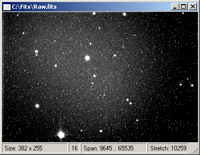
Raw image is affected by thermal noise and uneven field
illumination The purpose of dark frame subtraction was already
explained—elimination (or at last
reduction) of thermal noise. CCD dark current is proportional to
temperature. Thermal noise doubles every 6 or 7 °C, depending on the chip architecture. For
instance the Kodak KAF-0400 has dark current doubling temperature
6.3 °C. The charge
accumulated in pixels is also proportional to exposure time (dark
current is expressed in electrons per pixel per second at the
defined temperature). To reduce image thermal noise, the dark
frame subtracted from image should be obtained at the same
temperature for the same time as is the image itself.
Dark frame corresponding to the raw image above (left)
and the result after its subtraction (right) If the dark current depends linearly on temperature and
exposure time, it is possible to calculate dark frame from other
dark frames taken at different temperature and/or exposed for
different time. Some software packages require one dark frame
exposed for zero time (and call it bias frame), other software
does not require any special exposure times. Just take two dark
frames at different temperatures and the software interpolates
dark frame for required temperature. The same is true for the dark
frame exposition time.
Telescope field of view is often illuminated
non-uniformly—image intensity on the
borders can be lower than in the center, e.g. thanks to the
smaller telescope secondary mirror. Also dust particles on filter
or CCD camera window creates ring-like shades. All these effects
alter image brightness and cause not only aesthetics artifacts,
but also reduces measurement precision. It is possible to
eliminate these effects by applying flat field image.
Flat field corresponding to the raw image above (left)
and the result after flat field correction (right) Flat field image is an image of uniformly illuminated area.
Thus all image brightness variations on flat field are caused by
telescope or camera, not by the object we image. Ideal flat field
values are around one half of the image scale (average pixel count
should be around 32,000 for 16-bit cameras).
Applying flat field means dividing every image pixel with the
appropriate pixel of the flat field. Image pixels brighter due to
telescope or camera non uniformity are divided by bigger flat
field value, also brighter due to same reasons. But such division
changes image scale so we also multiple each pixel by flat field
average pixel value. If the operation is performed on integer
values, multiplication must precede division of course, else the
precision lost during integer division would destroy the
image.
|
