|
G2CCD-0400 camera is equipped with ordinary SLR camera lens,
pointing to the microscope screen in the ultra high vacuum chamber.
Camera is attached to the microscope body using custom-made arm.
Exposure times vary within seconds, so it is not necessary to cool the
CCD chip below freezing point—the KAF chip
generates approx. 1 electron per second per pixel at 0 deg.C.
G2CCD-0400 Camera on the Field Emission
Microscope Experiment results
The following images show the progress of experiment focused to
examination of growth and thermal stability of very thin palladium
layer on the tungsten sample covered by tungsten oxide. The sample
is prepared from 0.2 mm thin tungsten wire etched to very sharp
tip.

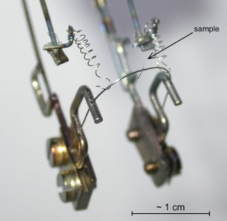
The sample holder with tungsten tip prepared for
experiment The images below show field emission images of the tip during
experiment. Field of view covers 800 nm (0.000,8 mm) diameter—camera
shows approx. 1.5 nm
per pixel. All images are displayed in false colors to enhance
subtle details.
The first figure shows the clean surface of the tungsten
monocrystal.
The second frame shows the sample surface after mild
oxidation.
Then a very thin layer—only
0.3 nm—of palladium is evaporated on the tungsten oxide
surface cooled to 78 K.
The sample is then heated to approx. 350 and 500 K. After heating to 350 K (left image) palladium layer forms island
with cross shape influenced by tungsten oxide support. Additional
heating to 500 K (right image)
probably cause encapsulation of palladium by tungsten oxide (the
image is similar to bare oxidized tungsten before palladium
evaporation).
All images on this page are courtesy of Ing. Jan Plsek, PhD.,
J. Heyrovský Institute of Physical Chemistry, Prague
| 